The invention of the transistor in December 1947 marked the beginning of a new age in electronics, one in which computers, mobile phones, the Internet, and almost all other electronic devices would not exist without transistors. This semiconductor component has had as much of an impact on technology, society, and daily life as the invention of the wheel or electricity. Let’s have a look at the invention and history of the transistor.
Transistors, in the form of integrated circuits and microchips, can be found in almost every modern electronic device. They are responsible for producing the ones and zeros that are the basis of all digital devices. Simultaneously, they serve as amplifiers, oscillators, and in numerous other fundamental roles in contemporary electronic devices. There were some radical innovations and some detours in the early stages of the development of transistors.
From the vacuum tube to the transistor
The transistor is a really revolutionary development, on par with the wheel and the discovery of fire. It has had maybe the greatest impact on our daily lives and our whole society. Without it, we wouldn’t have desktop computers, laptops, mobile phones, the Internet, or anything else that relies on a microprocessor. Calculator-powered computers would still take up a whole room.
A combination of a switch, rectifier, and amplifier

Most electronic parts and gadgets rely on electrical circuits, which determine whether or not a current flows and under what circumstances. But to do this, you’ll need switches that can be operated by electricity. The flow of a considerably greater current is controlled by a much smaller control current. A computer’s ability to perform digital computing tasks is based on the combination of these switches, or “logic gates,” into circuits. However, this can only be achieved if the electrical switches are very responsive and can be regulated accurately.
In addition, many technological applications need the amplification and modification of electrical signals, such as the production of radar or radio signals, the use of loudspeakers, microphones, and monitors, and the transformation of alternating current (AC) to direct current (DC). Again, the goal is to control the resultant electrical current flow in the most efficient and cost-effective method.
When vacuum tubes were first used

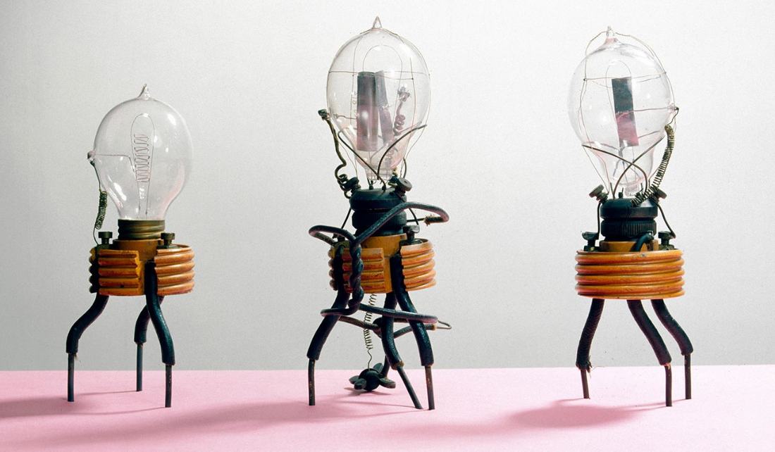
Mechanical switches in the form of relays were employed for these purposes before the invention of the transistor, but they switched between states slowly. Alternatively, vacuum tubes, which were first developed in 1904, were put into service. They are so-called triodes and are constructed out of an airtight glass, steel, or ceramic tube with three electrodes. With the third electrode in place, the electric field created between the anode and cathode can be used to control the amount of current flowing between the two.
However, vacuum tubes have a number of drawbacks, including their bulk, fragility, and high power requirements for regulation. Cabinets full of vacuum tubes were utilized for the circuits in the early computers, which meant they took up whole rooms. The British employed a machine called Colossus to decipher German signals during WWII. Meanwhile, the Americans were hard at work on ENIAC, the first general-purpose computer. Similarly, the vacuum tubes within the popular tube radios of the day made the receivers seem more like pieces of furniture than portable listening devices.
Another drawback is that the switching speed of tubes is restricted. This is despite the fact that they switch significantly quicker than mechanical relays. The need for rectifiers and amplifiers that could switch in the gigahertz range arose as a pressing issue, particularly during World War II, when the military’s radar systems were upgraded to greater power.
The discovery of semiconductors

Scientists and engineers set out to find a replacement for the fragile and cumbersome vacuum tubes that were the source of these issues. Within this context, semiconductors gradually came to the forefront. Depending on the temperature, chemical makeup, and orientation, these materials may either be insulators or conductors.
In 1874, German scientist Karl Ferdinand Braun noticed that these crystalline solids displayed a rectifier effect. “In a large number of natural and artificial sulfur metals, […] I found that their resistance varied with the direction, intensity, and duration of the current.” When an alternating voltage was supplied, electrons could only flow through the material in one direction, producing a direct current at the opposite end.
The concept of the field effect transistor
As a result of these discoveries, engineers created the first diodes in the 1920s using lead sulfide and copper oxide. They were used in a variety of radio receivers. By adding a third electrode, a semiconductor diode can function like a vacuum tube’s triode, as first described by scientist Julius Lilienfeld in 1925. He dubbed the apparatus a field-effect transistor (FET) because of the fact that the electric field affects the semiconductor’s current flow.
Unfortunately, no practical implementations of semiconductor triodes were successful thus far. Until recently, very little was understood about the physics at play inside semiconductors. Also, the metal oxide or metal sulfide semiconductors employed back then were chemical compounds, and the wide variations in their crystalline structure and electrical characteristics during production made them unsuitable for usage. In the end, the quest for crystalline vacuum tube replacements appeared fruitless.
The first approaches for transistors
The transistor wouldn’t exist without the discovery of semiconductors like germanium and silicon. They, along with many other electronic components, owe their existence to the crystalline solids’ unique electronic characteristics. There is a good reason why the semiconductor sector has become a multibillion-dollar, internationally competitive industry.
What matters is the bandgap

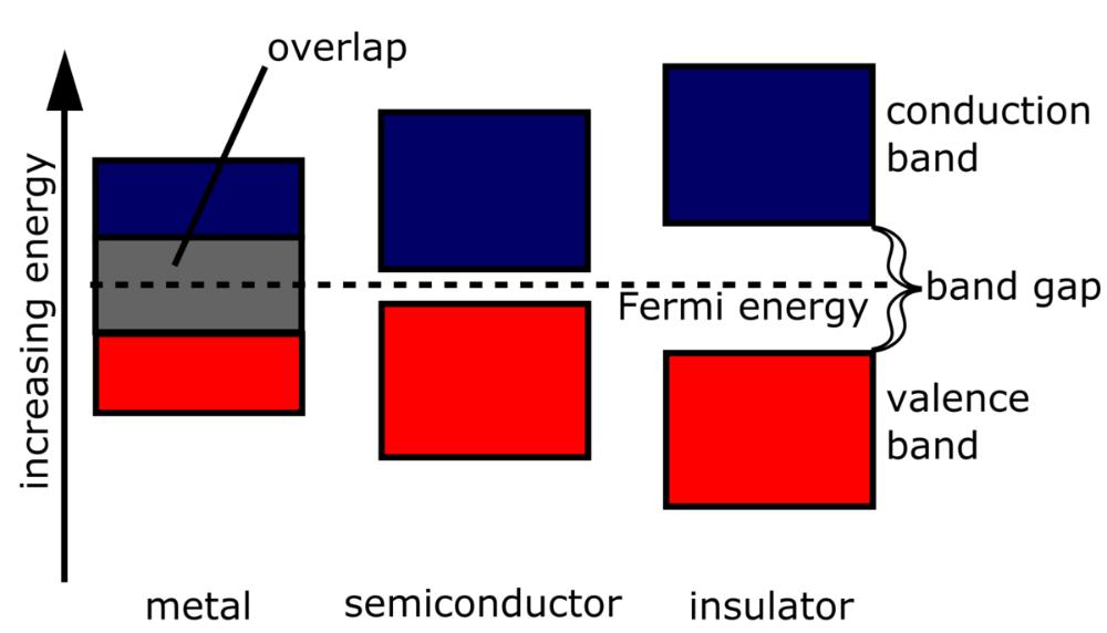
Beginning in the late 1930s, semiconductors started their meteoric rise to prominence. Around this time, researchers had finally figured out the atomic-level causes of a semiconductor’s inconsistent electrical conductivity. They found that, unlike in metals, the electrons in these substances are restricted in their initial positions. Rather, the semiconductor electrons need to be stimulated to a particular level before they get excited and transition into the mobile state.
Semiconductors have a band gap of 0.1–4 electron volts (eV) between their insulating valence band and their mobile conduction band. When electrons in the semiconductor get energy in the form of heat, radiation, or electric current, they are able to jump the band gap. The semiconductor characteristics of substances are at their best when their atoms each contain four valence or outer electrons. Compounds like cadmium sulfide and gallium arsenide, as well as the elements silicon and germanium, fall within this category.
The effect of impurity
Also noteworthy is the discovery that germanium’s and silicon’s electrical characteristics can be tailored by the strategic introduction of foreign atoms into their crystal lattices. This doping results in either an excess of electrons (n) or a surplus of positively charged vacancies (p) in the crystal lattice, depending on the kind of impurity. Since the band gap is narrowed by the presence of these surplus local charges, the semiconductor’s local conductivity can be enhanced.
However, it was not feasible to create silicon and germanium crystals of adequate purity until after World War II, which was a necessary requirement for the fabrication of tailor-made doped semiconductors. The availability of semiconductors with a purity of 99.999 percent was only made possible by developments in crystal growth.
The attempt for the first transistor

As a result, several laboratories, including the illustrious Bell Laboratories in New Jersey (home to the R&D division of a major U.S. telephone corporation), began experimenting with doped germanium and silicon semiconductors. In 1945, Bell Labs’ vice president, Mervin Kelly, began a research effort to find an alternative to vacuum tubes that could be made from semiconductors. His choice of leaders for the cross-disciplinary team included physicist William Shockley and chemist Stanley Morgan.
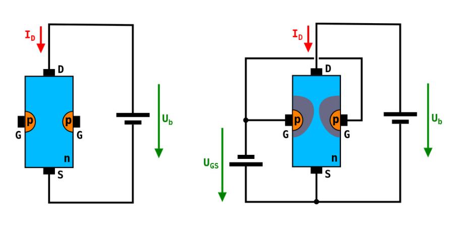
Shockley and his colleagues began testing out various configurations of two semiconductor layers with variable doping levels as part of this effort. They employed an external electric field in the form of a third electrode, similar to what Lilienfeld had described before it, to affect the current flow between two electrodes (source and drain) inside the material. To do this, the controlling gate electrode must be situated in an n-doped area of the semiconductor, in contrast to the drain and source electrodes, which must be situated in a p-doped zone.
The current flowing between the two other electrodes is restricted and regulated by the voltage provided to the gate electrode, which creates an exclusion zone in its vicinity. The current flow between the source and drain electrodes can be modulated by varying the size of the non-conducting exclusion zone, which acts like a lock gate. These days, we refer to this basic kind of field-effect transistor by its more modern name, a junction field-effect transistor (JFET).
Two independent groups
In 1945, Shockley and his colleagues produced a germanium-based junction field-effect transistor, but the external field’s modulating effect was too weak for practical application. Therefore, Shockley tasked two members of his semiconductor research team, John Bardeen and Walter Brattain, with digging more into the matter. He, too, originally looked elsewhere for answers.
On the other side of the Atlantic, two German physicists named Heinrich Welker and Herbert Mataré were tackling the same issue and, like their American counterparts, were successful in putting the principle into practice for the first time in 1945 by experimenting with precursors to the junction field-effect transistor. Unfortunately, the expected results were still too modest, just as they had been for Shockley and his group.
The two groups were now developing more effective transistor technology apart from one another.
Toward the first transistor
It seemed like a major development was on the horizon by the autumn of 1947. John Bardeen and Walter Brattain, two semiconductor researchers working at Bell Labs in New Jersey, had identified the root cause of the early transistor experiments’ failure. Their group’s transistor models, despite some promising methods, stubbornly refused to operate, responding only very weakly to the applied control field.
The scientists found that the early versions of field-effect transistors had insufficient semiconductor penetration for the regulating electric field of the control electrode. This field regulates the flow of electricity, and its failure meant that the “lock gate” was not working as intended. Instead, the material’s electrons were trapped in a thin barrier layer just below the surface. Because of this, the candidate transistor could no longer benefit from the regulatory action.
A plastic wedge, gold foil, and germanium

Brattain and Bardeen started tinkering with a new building approach to see if they could find a workable answer. In this instance, a germanium plate was set above a metal base. This was n-doped, meaning that it had an abnormally high concentration of free electrons brought about by the incorporation of a foreign element, most often phosphorus or arsenic. Afterward, a very thin layer of p-doped germanium was grown on top. Boron and other alien atoms flooded this layer with “holes,” or a plethora of positive charges.
The aha moment finally arrived when Brattain and Bardeen came up with the idea of using a triangular plastic wedge linked to a spring and then wrapping it all in gold foil. They created two closely spaced contact points by scoring the conductive gold foil at the wedge’s tip. These were now suitable for use as two separate electrodes, with each one connecting to a separate circuit through its conductive metal base.
The first test of Brattain and Bardeen’s transistor model was performed on December 16, 1947, at their lab. It functioned, with a weak current flowing from the emitter side of the gold tip to the base and a corresponding change in the current flow in the second circuit, the latter of which was dependent on the amount of current provided to the first gold electrode.
The device worked as a variable switch and amplifier, increasing the input signal by a factor of a thousand, precisely as expected. After doing “the most important experiment” of his life, Brattain informed his team on the way home that night. But he didn’t say what it was just yet.
The first functional transistor

On December 23, 1947, the two scientists finally showed their discovery to Bell Labs’ upper management. They used a microphone and a loudspeaker to show off the transistor’s amplification capabilities during the internal demonstration. The microphone was hooked up to the little circuit of the emitter electrode, while the loudspeaker was linked to the second circuit. This meant that the speaker had to faithfully duplicate the original sound in order for the transistor to have worked.
It was at this point that Brattain and Bardeen realized their dream of creating the first operational transistor. Finally, a semiconductor-based miniaturized component to replace bulky vacuum tubes has been created. At a press conference held by Ball Laboratories on June 30, 1948, the two scientists revealed their new invention to the world.
The double-point contact transistor
The point-contact transistor is based on the basic design idea pioneered by Brattain and Bardeen. These bipolar transistors differ from the prevalent field-effect transistors in that both positive and negative charge carriers participate in the amplification process. To rephrase, the “holes” and the “electrons” in the semiconductor are both activated or mobilized.
In 1951, mass-produced point-contact transistors were used in the construction of a variety of products including telephone switchboards, hearing aids, oscillators, and even the first prototypes of television sets. These devices were the quickest switching transistors available up to 1953. In 1956, Brattain and Bardeen were honored with the Nobel Prize in Physics for their work on this.
Aside from the two American scientists, two German physicists, Herbert Mataré and Heinrich Welker, independently developed a very similar concept to the point-contact transistor without knowing about the progress being made at Bell Labs. Similarly, they built a functional point-contact transistor in 1948, although they were behind the competition.
The first bipolar transistor

In 1947, two American scientists named John Bardeen and Walter Brattain devised the first point-contact transistor, and it was a significant advancement in electronics but not yet practical as the backbone of electronics and the foundation of the first computers. As a result of their thinness, the “point-contact” electrodes tended to break easily. The essential charge carriers in this transistor only flowed across a narrow region on the semiconductor’s surface, hence the amplification it could provide was poor.
However, this all changed with the invention of the bipolar junction transistor (BJT) at Bell Labs in New Jersey only six months later. After William Shockley’s original attempts to create a field-effect transistor device in 1945 were unsuccessful, he went on to construct this new device. In the first presentation of Brattain and Bardeen’s point-contact transistor, Shockley was left out. To his dismay, he was not credited as a co-inventor on the patent for the first transistor and did not play a significant role in its creation.
The fact that he wasn’t an “inventor” dampened his enthusiasm for the team’s accomplishments. “I was frustrated that my own efforts, which had after all been going on for eight years at the time, had not resulted in any significant invention.” But that was about to change.
Shockley had been studying the physics of p-n junctions in semiconductors, the activities that take place at the interface between the two differentially doped semiconductor zones, for a few months prior to this. The scientist was trying to find a method to improve the device so that charges could be transported farther than just over its small surface. Shockley created the first working transistor on New Year’s Eve, 1947, in a hotel room in Chicago.
Stacked layers

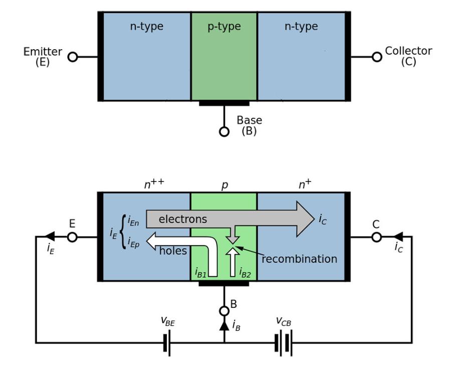
The scientist created a sandwich out of three layers of germanium, which was the main innovation. A thin n-layer was sandwiched between two p-doped layers, or vice versa. Applying a voltage to the thin intermediate layer in such a surface transistor reduces the barriers at the n-p junctions of the semiconductor. Therefore, there is no longer any impediment to the free flow of electrons from one n-zone to the other, while positively charged holes from the p-layer can now move in the opposite direction.
Bipolar transistors were far more powerful amplifiers than point-contact transistors because they worked on a different operating principle. Plus, they were more durable. Bell Labs had filed for a patent on the transistor a few days before Shockley’s public unveiling of it at a press conference on June 30th, 1948.
Even though it wasn’t the first fully working transistor, the bipolar transistor was a major step forward for semiconductor technology and ultimately modern electronics. These reliable parts, which were simple to standardize because of advances in crystal-growing techniques, found quick adoption in applications requiring either high-speed circuits or substantial amplification. Along with John Bardeen and Walter Brattain, Shockley won the Nobel Prize in Physics in 1956 for his work on the bipolar transistor.
With their combined efforts, the three physicists sparked a wave of invention that would permanently alter the state of the art. The invention of the transistor has far-reaching consequences for our culture and economy. After all, it was because of their efforts that electronics and computer technology were able to be shrunk down to more manageable sizes.
However, a crucial step was still lacking at the dawn of the digital era.
The beginning of the silicon era
However, the shift to silicon, the semiconductor used in almost all modern electronic circuits, still remained to be achieved. It’s because most transistors in the 1950s and 1960s were fabricated from monocrystalline germanium. The lower melting temperature of this element makes it more amenable to processing, and the rapid movement of charge carriers inside the crystal lattice allows for rapid switching times.
The problem with germanium

However, germanium does have a few drawbacks when used as a transistor material. This semiconductor’s bandgap is just 0.64 electron volts, which results in undesirable leakage currents. Once the temperature rises above around 167°F (75°C), the thermal energy is enough to make the material conductive. That’s why germanium transistors can’t be used at temperatures higher than that, since they stop switching. However, silicon is far more reliable; transistors constructed of silicon can operate at higher temperatures because of their bigger band gaps.
The difficulty in creating high-purity monocrystalline blocks of silicon stems from the material’s greater melting point of 2,580°F (1,415°C) and its increased reactivity. The electrical performance of the crystal is negatively impacted since the molten silicon reacts with practically every crucible, including quartz glass. Thus, it was initially quite difficult to manufacture silicon semiconductors with the necessary purity and doping.
Race to create the first silicon transistor
In 1954, researchers finally succeeded in overcoming these obstacles, and again, this occurred twice independently but almost simultaneously. The chemist Morris Tanenbaum at Bell Labs developed a process by which the doping rate of the silicon could be controlled while the single crystal was being pulled out of the melt. Thus, on January 26, 1954, the team developed the first n-p-n silicon transistor that had a reliable amplification performance. Bell Labs, however, initially chose not to share or patent this discovery.
Simultaneously, Gordon Teal, a chemist who had previously worked at Bell Labs, was developing a method at Texas Instruments to create silicon semiconductors with the needed characteristics. Because of this lack of purity, Teal’s team devised a method to make the interlayer of the transistor sandwich exceedingly thin, on the order of 25 micrometers. As a result, the semiconductor’s charge carriers were able to traverse this barrier, despite the presence of certain impurities. A functional n-p-n silicon transistor was developed on April 14, 1954.
Silicon has replaced germanium as the dominant semiconductor in modern transistors.
A new age
“Contrary to what my colleagues have told you about the gloomy prospects for silicon transistors: I have several of them in my pocket right now,” Teal said at a technical conference on May 10, 1954, marking an early presentation of his new silicon transistor. This was in stark contrast to Bell Labs’ decision not to announce their breakthrough.
Teal then provided a concrete example of the benefits of these components by submerging a germanium transistor attached to a loudspeaker in hot oil, at which point the music abruptly stopped. He then tried it using a silicon transistor, and the sound remained intact. The PR stunt was successful; the Teal technique was adopted, in part because the rival method was more difficult to standardize. That’s how Texas Instruments got the ball rolling on mass-producing silicon transistors.
It was this discovery that ushered in the “silicon age” and paved the way for the explosive growth of the computer and semiconductor industries. New transistor designs allowed for mass manufacture, downsizing, and integration into integrated circuits, and silicon transistors gradually displaced older germanium devices during the 1960s and 1970s.
These semiconductors made it possible to carry about and operate on computers anywhere, and they also powered global communication infrastructure. The transistor’s reputation as the “nerve cell” of the computer age is well-deserved. It’s safe to say that life as we know it now couldn’t exist without the invention of the transistor.


